1. Introduction
he Viterbi Algorithm [1] [3] [16] is used widely for estimation and detection problems in digital communication and signal processing. It is used to detect signals in communication channels with memory [3], and to decode sequential error control codes [16] that are used to improve the performance of digital communication systems. During the transmission or storage process, the digital data may get corrupted due to noise. Channel coding [1] is a method to encode the data in a manner that it can be recovered even if it gets influenced by noise .Channel Coding involves adding redundant bits [3] to the data so that when it gets corrupted due to noise, the data can still be recovered through the redundancy [1] present in it. Block codes and convolution codes [16] are two major forms of Channel coding. The block codes [16] transform a block of k symbols into a block of n symbols called code word, where n > k. Since the output n-symbol code word depends only upon the corresponding k-symbol input code word, the encoder is memory less and can be implemented in a combinational logic. On the other hand, a Viterbi encoder [3] [16] not only depends on the corresponding k-symbol input block but also on m previous input blocks. Viterbi encoders are implemented in sequential logic because they are associated with memory element. Keeping in mind the essentials of communication channels in wireless systems, reliable data communication, fast as well as accurate is the main requirement and Viterbi coding helps us in achieving the same. The Viterbi algorithm [1] applies the maximum-likelihood path [3] [16] method for error detection. The most common metric used is the branch distance metric [1]. This is basically the dot product between the received codeword and the allowable codeword [16]. These metrics are cumulative so that the path with the largest total metric is the final desired output. The selection of survivor path basically determines the whole of the Viterbi algorithm and ensures that the algorithm completes with the maximum likelihood path [1]. The algorithm ends and is completed when all of the nodes in the trellis have been labeled and their entering survivor paths have been determined. The design space for VLSI implementation of Viterbi decoders is large, involving choices of throughput, latency, area, and power. Even for a fixed set of parameters like constraint length, encoder polynomials [3] and trace-back depth [1], the task of designing a Viterbi decoder is quite complicated and requires significant effort. Sometimes, due to incomplete design space exploration or incorrect analysis, a suboptimal [3] design is selected In onchip interconnects [2] [4], there is propagation delay [5] due to resistance and inter wire interconnects and gates and some others sources are such as alpha particles, electromagnetic interference [2] and power grid fluctuation [8]. Various techniques are used to minimize the delay and also various error detection and correction scheme [6]. In this paper, a Spatio-temporal bus encoding scheme [2] [4] [5] [9] is proposed which are reduced the delay due to its optimized hardware parameters and implementation. Experimental results of this scheme is show that this scheme perform better and have advantages of error detection, also in this paper we compare this scheme with Viterbi encoding scheme.
2. Year
The rest of this paper is organized as follow. The algorithm of Spatio temporal scheme is proposed in section II. The algorithm of Viterbi encoding scheme in presented in section III. Section IV the presents the simulation results, RTL views and discussion part. Comparative analysis of Synthesis report and timing parameters are listed in section V.
3. II.
4. Spatio Temporal Bus Encoding & Decoding
Spatio encoding [12] is applicable for arbitrary bus encoding .This techniques are proposed for 8 bits, 16 bits or ' N' bits data. Spatio temporal bus encoding scheme is proposed for eliminates the crosstalk classes [11] [13] for large energy consumption and delay of the buses [12]. This scheme is also designed to have builtin error detection [10] with very less circuit overhead. The architectures for the encoder and decoder circuit of the Spatio temporal encoding scheme are given in figure 1(a) and 1(b). The architecture of the Spatio encoder is proposed for scheme an 8 bits data bus. In the encoder which have data d t and previous encoded data E t-1 . There are two multiplexers [11] which have 3 common inputs from data d t and two XOR gates. It's output is E t and E t+1 . The data sent on the bus at time instance t-1 is stored in a register of 9 bits. It is denoted by E t-1 . The present data is stored in register which are denoted by d t . First multiplexer (2 x 1) has two inputs which are common may be any one bit of data d t (1), d t (2) and d t (3). The selection line of this multiplexer is directly configured as XOR output [12] of d t ( 2) and E X-1 (2). The output of this multiplexer is common input [13] [14] for E t ( 1), E t ( 2), E x (3), E x (4). Another multiplexer also has common inputs lines which are d t (5), d t ( 6) and d t (7) followed by XORed selection line of d t ( 6) and E t-1 (8). The decoding method for the proposed scheme is similar [15]. In decoding scheme [2] [12] [15] the original data d t is reconstructed from E t and E t+1 . Where E t+1 and E t are the input to the decoder and d t is obtained by the decoding algorithm. The first three bits of d t (1), d t (2) and d t (3) are common output of first multiplexer. This multiplexer accepts common input of E t (1), E t ( 2) and E t (3). E t+1 (3) is the selection logic of this multiplexer. First bit of E t+1 (1) is directly configured with d t (4). Another multiplexer accepts common inputs of E t ( 7), E t ( 8) and E t (9). Selection logic of this multiplexer is E t+1 (9). The output of this multiplexer gives the values of d t (5), d t (6) and d t (7). d t ( 8) is directly configured with E t+1 (7). For an example, consider an 8-bit data bus [2] for which encoded data will be of 9-bit length. Let the data be already available on the bus (9 bit) [ . Here transaction 0-1, 1-0 and 1-1 are represented by .
III.
5. Viterbi Encoding & Decoding
Conventional codes are helping to analysis the Viterbi algorithm [3]. Viterbi algorithm are supported by two steps, the initial step is to select the trellis from the bits that are achieved at the input at the receiver. A simple trellis [1] show with 4 stage points for transmission, each state is represented with a dot and The Encoded vector Hence the value of first encoded vector is 101. Similarly second bit form MSB is entered in shift register, second bit interval E 1 =1, E 2 =1, E 3 =0. Vector corresponding to second bit is Hence the value of second encoded vector is 101. In the same manner encoded vectors [1] [16] for other bit intervals can be found. The register will reset at seventh bit interval because maximum condition [16] of reset is (L+K= 4+3= 7). The output at each bit interval consists of V bits. Thus for each message there are (L+K) encoded vectors in the output code word. In the given table the coded output bit stream for all input data stream for encoder. Similarly, the encoding of 8 bit can understand. Considering and 8 bit input stream 10111010. Initially shift register contents are 000. First bit of MSB is entered in shift register then E 1 =1, E 2 =0, E 3 =0 the first encoded vector calculation Hence the value of first encoded vector is 101. Similarly second bit is entered from MSB, the contents of shift register will be E 1 =0, E 2 =1, E 3 =0, the conceded vector Hence the value of second encoded vector is 110. The register will reset at seventh bit interval because maximum condition of reset is (L+K= 8+3= 11). In the same manner encoded vectors for other bit intervals can be found and the encoded vectors are 11. Table 2 lists the values of encoded vectors for 8 bits input data stream. The Viterbi algorithm applies the maximumlikelihood principle [3]. The most common metric used is the Hamming distance metric [1]. This is just the dot product between the received codeword and the allowable codeword. These metrics are cumulative so that the path with the largest total metric is the final winner. The selection of survivor path is the main feature of the Viterbi algorithm and ensures that the algorithm terminates with the maximum likelihood path. The algorithm terminates when all of the nodes in the trellis have been labeled and their entering survivor paths are determined [16]. IV.
V = [V 1 V 2 V 3 ] in which the values of V 1 , V 2 and V 3 of the adders are V 1 = E 1 XOR E 2 , V 2 = E 2 XOR E 3 , V 3 = E 1 XOR E 3 .?? 1 =1 ? 0 = 1, ?? 2 = 0 ? 0 = 0, ?? 3 = 1 ? 0 = 1 ?? 1 = 1 ? 1 = 0, ?? 2 = 1 ? 0 = 1, ?? 3 = 1 ? 0 = 1 ?? 1 = 1 ? 0 = 1, ?? 2 = 0 ? 0 = 0, ?? 3 = 0 ? 1 = 1 ?? 1 = 0 ? 1 = 1, ?? 2 = 1 ? 0 = 1, ?? 3 = 0 ? 0 = 0 Global Journal of6. Simulation Result & Discussion
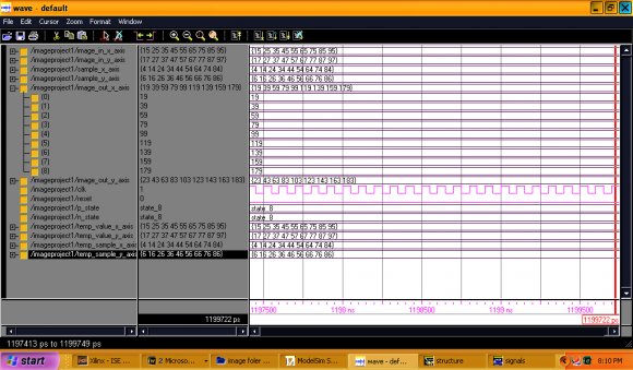
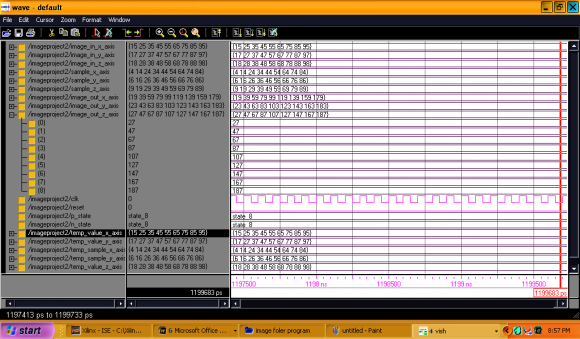
The snapshot shown in figure 4 3 explains the role of pins and their functions.
7. Comparative Analysis
Comparative analysis of Spatio and Viterbi encoding and decoding Schemes can be done by the timing parameters and device utilization summary extracted from Xilinx. Device utilization summary is the report of used device hardware in the implementation of the chip such as RAM, ROM, slices, flip flops etc. Synthesis report shows the complete details of device utilization as total memory utilization. If synthesis report does not have the optimized hardware, further chip development can be done in the Xilinx ISE design software.
The device targeted for synthesis on SPARTEN-3E FPGA .Timing parameters are synchronized with the clock signal. Timing details provides the information of net delay, minimum period, minimum input arrival time before clock and maximum output required time after clock. Table 4 compares the hardware utilization for Spatio and Viterbi Encoders. Table 5 compares the hardware utilization for Spatio and Viterbi decoders. Table 6 shows the timing parameter of Spatio and Viterbi Encoders and decoders. The memory utilization graph is shown in figure 8
8. Conclusion
The hardware chip for Viterbi encoder and decoder, Spatio encoder and decoder is implemented in Xilinx 14.2 and functionally checked in Modelsim 10.1b software. A comparative analysis is done with respect to hardware and timing parameters. In the chip implementation, it is analyzed that Spatio encoding and decoding is having less delay in comparison to Viterbi encoding and decoding. Memory utilization is less which is 1.75 % for Spatio encoder 4.33 % for Spatio decoder in comparison to Viterbi encoder and decoder. But there is a reduction of 48 % in combinational path delay in Spatio encoder and 42 % in Spatio decoder in comparison to Viterbi encoder and decoder. Hence Spatio encoding and decoding scheme is faster in comparison to Viterbi encoding and decoding.
9. Global

![â??"?â??" ?? ?? ? ? ? ? ? ??? ?? ?, â??" ?????? ? the state transition is shown as edge of branch. Each branch is known as the branch matrix. The use of trellis structure [16] is to find the coded sequence in transmission signal. Considering a Viterbi encoder as shown in figure 2, with three modulo-2 adders, which accepts the 4 bits data stream. Let, K = No of the shift registers = 3 V= No. of bits in the code blocks = 3 L= length of input data stream = 4.](https://computerresearch.org/index.php/computer/article/download/202/version/100589/1-Comparative-Analysis-of-Spatio_html/9334/image-3.png)
![Figure 2 : Viterbi Encoder [16]](https://computerresearch.org/index.php/computer/article/download/202/version/100589/1-Comparative-Analysis-of-Spatio_html/9335/image-4.png)
![Initially, it is assumed that the shift register is clear means the contents of [M 1 , M 2 , M 3 = 000]. Let the 4-bit data is 1101. The data stream is entered in the shift register from MSB. MSB bit of input data stream is entered into shift register and there is one bit right shift. Thus at first bit interval is E 1 =0, E 2 =1, E 3 =0. So the vector corresponding to first bit is determined by the calculation, .](https://computerresearch.org/index.php/computer/article/download/202/version/100589/1-Comparative-Analysis-of-Spatio_html/9336/image-5.png)
![Figure 3 : Trellis diagram of decoding logic [1]](https://computerresearch.org/index.php/computer/article/download/202/version/100589/1-Comparative-Analysis-of-Spatio_html/9337/image-6.png)


| Input data stream | Coded output bit stream | |
| 0000 | 000 000 000 000 000 000 | 000 |
| 0001 | 000 000 000 101 110 011 | 000 |
| 0010 | 000 000 101 110 011 000 | 000 |
| 0011 | 000 000 101 011 101 011 | 000 |
| 0100 | 000 101 110 011 000 000 | 000 |
| 0101 | 000 101 110 110 110 011 | 000 |
| 0110 | 000 101 011 101 011 000 | 000 |
| 0111 | 000 101 011 000 101 011 | 000 |
| 1000 | 101 110 011 000 000 000 | 000 |
| 1001 | 101 110 011 101 110 011 | 000 |
| 1010 | 101 110 110 110 011 000 | 000 |
| 1011 | 101 110 110 011 101 011 | 000 |
| 1100 | 101 011 101 011 000 000 | 000 |
| 1101 | 101 011 101 110 110 011 | 000 |
| 1110 | 101 011 000 101 011 000 | 000 |
| 1111 | 101 011 000 000 101 011 | 000 |
| Input data stream | Coded output bit stream |
| Year | |
| Pins | Functional Description |
| clk | Signal produce to Clock signal ( 1 bit of std_logic) |
| Reset | used for synchronization of the components by using clk ( 1 bit of std_logic) |
| Tx | 9 bit encoded data by Spatio encoder at time t |
| Tx_Minus | 9 bit encoded data by Spatio encoder at time t-1 |
| Tx_plus | 9 bit encoded data by Spatio encoder at time t+1 |
| dt | Input data of Spatio Encoder and output of Spatio Decoder (8 bits of std_logic_vector) |
| Data_stream | Input data of 8 bit for Viterbi Encoder (8 bits of std_logic_vector) |
| Encoded_vector_data | Array of Encoded data (0 to 10) for 8 bit data_stream(8 bits of std_logic_vector) |
| Decoded_data_stream | Decoded output of Viterbi decoder (8 bits of std_logic_vector) |
| Device part | Viterbi Encoder Used Available Utilization Used Available Utilization Spatio Encoder | |||||
| Number of Slices | 60 | 2448 | 2% | 1 | 2448 | 0 % |
| Number of Slice Flip Flops | 23 | 4896 | 0 % | 2 | 4896 | 0 % |
| Number of 4 input LUTs | 105 | 4896 | 2 % | 50 | 4896 | 1% |
| Number of bonded IOBs | 43 | 158 | 27 % | 46 | 158 | 29 % |
| Number of GCLKs | 1 | 24 | 4 % | 1 | 24 | 4 % |
| Device part | Viterbi Decoder Used Available Utilization Used Available Utilization Spatio Decoder | |||||
| Number of Slices | 34 | 2448 | 1% | 26 | 2448 | 1% |
| Number of Slice Flip Flops | 43 | 4896 | 0 % | 33 | 4896 | 0 % |
| Number of 4 input LUTs | 6 | 4896 | 0 % | 4 | 4896 | 0 % |
| Number of bonded IOBs | 18 | 158 | 11 % | 16 | 258 | 10 % |
| Number of GCLKs | 1 | 24 | 4 % | 1 | 24 | 4 % |
| Parameter | Viterbi Encoder | Utilization Viterbi Decoder Spatio Encoder Spatio Decoder | |||
| Minimum Period | 3.047ns | 2.058 ns | 1.578 ns | 1.567 ns | |
| Minimum input arrival time before clock | 8.515ns | 4.053 ns | 2.056 ns | 2.023 ns | |
| Maximum output required time after clock | 4.179ns | 4.179 ns | 3.0567 ns | 3.067 ns | |
| Maximum path delay | combinational | 12.014 ns | 10.057 ns | 6.232ns | 5.797 ns |
| Maximum Frequency | 325.165 MHz | 325.53 MHz | 325 .27 MHz | 325 .10 MHz | |
| Memory Utilization | 116408 kB | 115384 kB | 114360 kB | 110380 kB | |
| VI. |